Products

ApotheoTech sells the parts of a high-speed camera that are hard to build twice: the interface cores, the boards to run them on and the software that gets frames to an application. All of it came out of our own camera work, and the same parts are the starting point for custom designs.

IP cores

Interface cores for AMD FPGAs, written from the specifications. Three are proven in hardware and one is in development. Together they cover the path a frame takes through a camera: off the sensor, down the cable and onto a drive.

ShippingHardware provenBFM verified

CoaXPress 2.1 Host and Device

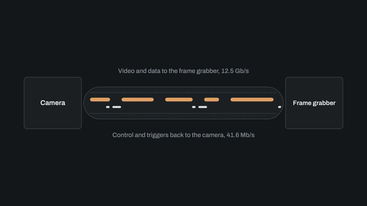
CoaXPress 2.1 cores for AMD FPGAs with GTH or GTY transceivers. The Host goes in a frame grabber and the Device goes in a camera. Both come from one code base, and both build for 1, 2 or 4 lanes of CXP-12, which is 12.5 Gb/s per lane.

Video moves on AXI4-Stream and control on AXI4-Lite. The Host reads and writes camera registers over the control channel. The Device carries the register bank and serves the GenICam XML. Hardware triggers are generated on the Host and decoded on the Device.

License either end, or license both and test them against each other on one board. Lane count is a build option, and a single-lane license costs less when 12.5 Gb/s is enough.

Included with a license

  • Encrypted netlist for your device and transceivers
  • Basic example design
  • Product brief and integration notes
  • One year of updates
Video bursts travelling down a coax cable while control words travel back
Line rate
CXP-12, 12.5 Gb/s per lane
Lanes
1, 2 or 4
Pixel formats
Mono, Bayer, RGB and YUV at 8, 10, 12 and 16 bit
Interfaces
AXI4-Stream video, AXI4-Lite control, trigger I/O
Proven on
ZCU106 and KCU116, with the APT-C11-FMC
Verified with
SystemVerilog BFMs in simulation
Resource use
Host, 1 lane of CXP-12: 5,592 LUTs, 7,309 registers and 6.5 BRAM
ShippingHardware proven

SLVS-EC RX

A receiver for Sony SLVS-EC image sensors on AMD FPGAs. It comes with two PHY options: the GTH, GTY or GTP transceivers, or plain HP I/O. Both run at Baud 3, and both are validated with the IMX530, IMX547 and IMX421.

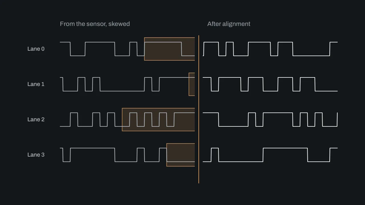
Each lane has its own PHY front end. The lanes are aligned and deskewed, packet headers are decoded with ECC, payloads are checked by CRC, and lines are rebuilt across lanes. Video leaves on AXI4-Stream, with control, status and per-lane error counters on AXI4-Lite.

The HP I/O option is for UltraScale and UltraScale+ designs whose transceivers are already spent on PCIe, CoaXPress or Ethernet. Lane count is a build option from 1 to 8. On the Aper-Oculus the core runs an IMX530 on 2 lanes at 3840 x 2160 and 30 fps.

Included with a license

  • Encrypted netlist for your device, PHY and lane count
  • Basic example design, with DisplayPort output on Zynq MPSoC targets
  • Integration notes
  • One year of updates
Four serial lanes arriving skewed and leaving aligned
Line rate
Baud 3
PHY
GTH, GTY or GTP transceivers, or HP I/O
Lanes
1, 2, 4 or 8
Sensors validated
IMX530, IMX547, IMX421
Proven on
ZCU106, KCU116 and Aper-Oculus
Resource use
1,433 LUTs, 2,835 registers and 4 BRAM, with AXI4-Stream out
Hardware provenBFM verified

NVMe host

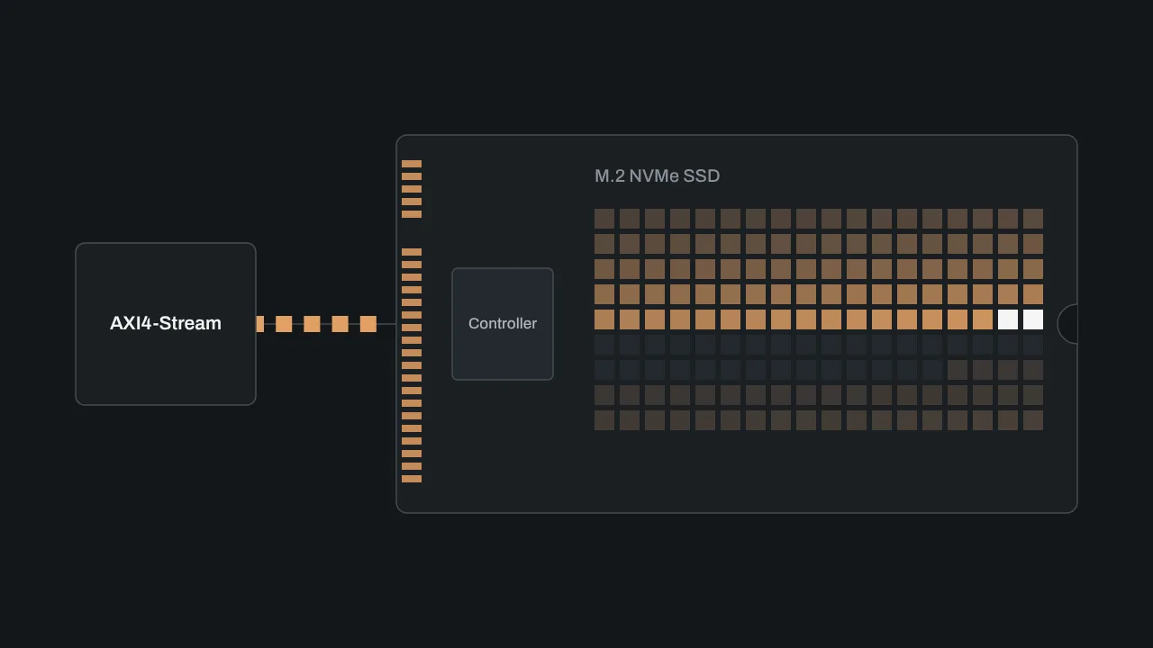
An NVMe host controller for AMD FPGAs that writes an AXI4-Stream straight to an M.2 SSD. No CPU and no operating system sit in the write path.

The core runs on its own PCIe root-port stack. The transaction and data link layers were written in house, so it is not tied to one hard block: it runs over AMD's PG239 soft PHY or the PG213 hard block. A queue engine builds PRP lists for long sequential writes and applies backpressure to the source when the drive stalls.

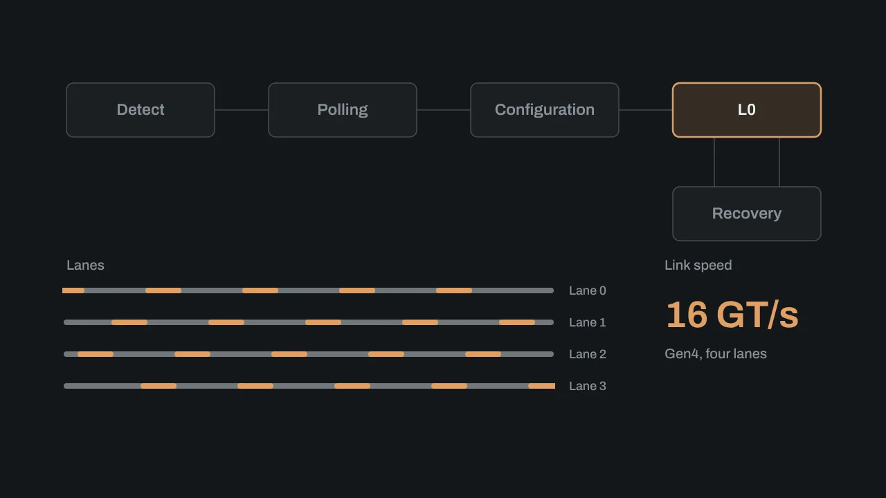
Choose the generation and the link width that fit the drive, the data rate and the transceivers you have left. A Gen4 x4 link carries up to 7.88 GB/s before protocol overhead, and a Gen3 x1 link 0.98 GB/s.

Included with a license

  • Encrypted netlist for your device, generation and width
  • Basic example design
  • Integration notes
  • One year of updates
A stream being written block by block to an M.2 drive
PCIe
Gen3 and Gen4
Link width
x1, x2 or x4
PHY
PG239 soft PHY or PG213 hard block
Interfaces
AXI4-Stream ingest, AXI4-Lite control
FPGA families
AMD UltraScale+
Proven on
ZCU106 and Aper-Oculus, on real drives
Verified with
A BFM in simulation
In development

PCIe Gen4 MAC for LitePCIe

The PCIe MAC that sits under the NVMe host core, packaged for LitePCIe. It drives AMD's PG239 PHY on UltraScale+ GTH and GTY transceivers and presents the interface LitePCIe expects from a hard PHY.

An existing LitePCIe design can therefore move to Gen4 without the hard PCIe block, and the rest of the design does not change. The transaction and data link layers are the ones that already carry the NVMe host core in hardware.

This core is in development. Early access customers help set the first supported configurations.

Included with a license

  • Encrypted netlist
  • LitePCIe integration example
  • One year of updates
A PCIe link training to L0, simplified
Targets
AMD UltraScale+
PHY
PG239 on GTH or GTY
Generations
Gen3 and Gen4
Interface
LitePCIe PHY port

Evaluation boards

The hardware the cores are developed and validated on. Buy one to evaluate a core on a known-good platform, or to start a camera design from a board that already works.

Aper-Oculus
SOM
AMD Kria K26 (Zynq UltraScale+)
Sensor interface
SLVS-EC, on board
Expansion
VITA 57.1 FMC
Sensors proven
IMX547, IMX530, IMX421
In the store, made to order

Aper-Oculus

APT-KRIA-FMC-02-SLVS, $1,150

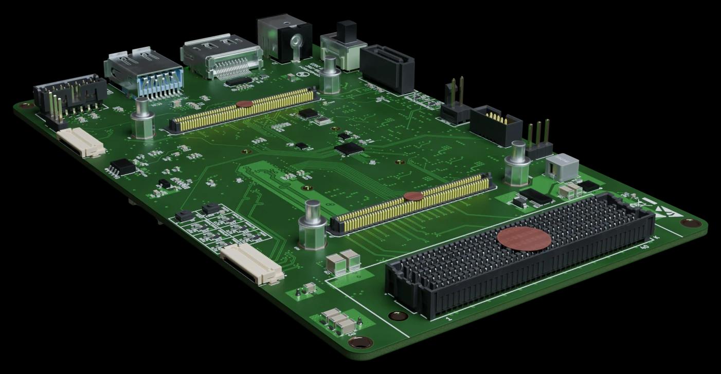
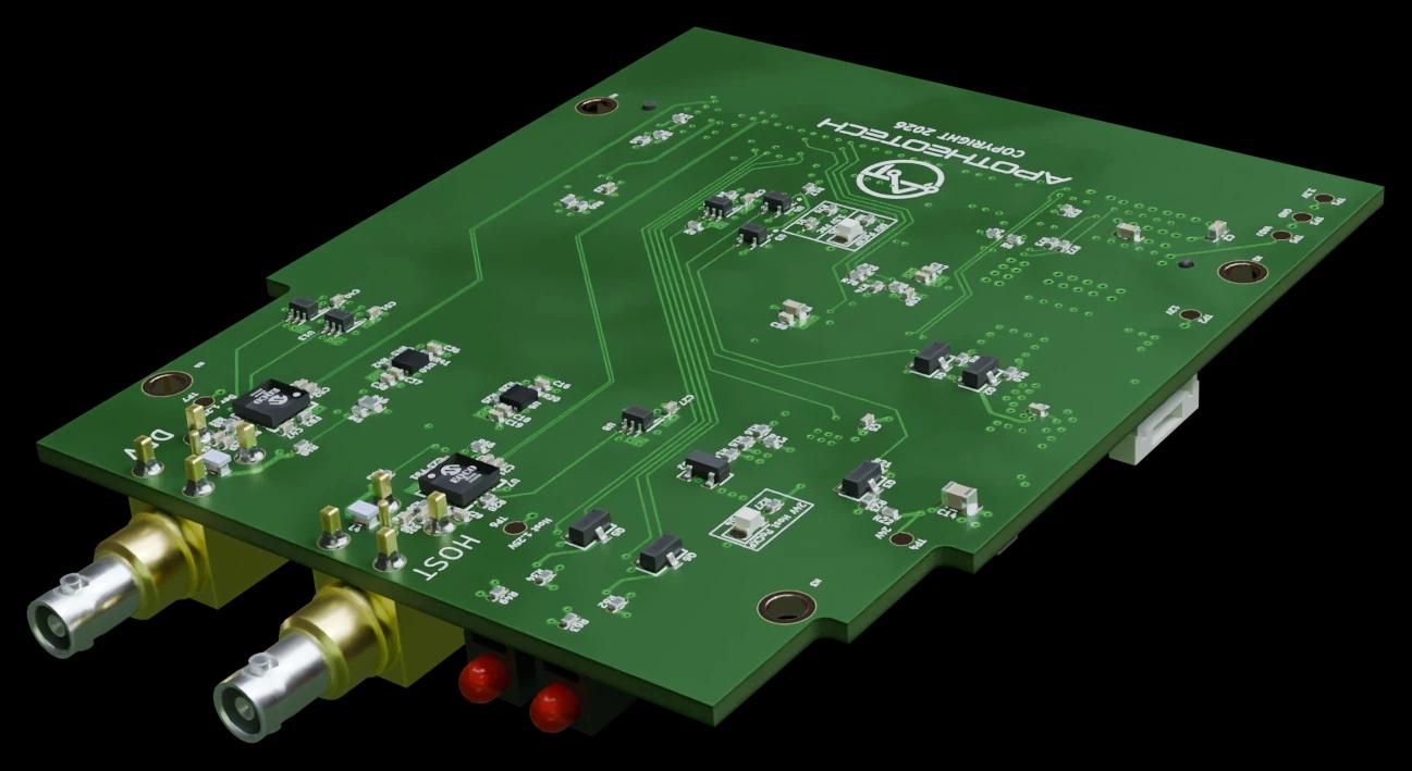
A carrier for the AMD Kria K26 SOM, built for high-speed camera work. It has an SLVS-EC sensor interface on the board, so a Sony sensor connects without an adapter card, and a VITA 57.1 FMC slot for expansion.

It is the reference platform for the SLVS-EC, CoaXPress and NVMe cores. Each of them has an Aper-Oculus example build, and every FMC card in the line is validated against this carrier, so an integration question has a known-good answer.

The SOM is socketed, so the compute module can be swapped without respinning the carrier. The board comes with reference designs, constraints and build scripts, bring-up notes and schematic-level integration support.

APT-C11-FMC, CoaXPress FMC
Lanes
1, transmit and receive
Line rate
Up to 12.5 Gb/s
Protocol
CoaXPress 2.1
Temperature
-40 to +85 °C
In the store

APT-C11-FMC, CoaXPress FMC

APT-C11-FMC-01, $850

One CoaXPress 2.1 lane on an FMC card, usable as Host or Device, at up to 12.5 Gb/s, with the equalizer and cable driver on the card. Power, data and camera control travel over one 75 ohm coaxial cable.

It is the card the CoaXPress cores are validated on. The free ZCU106 demo runs Host and Device in loopback on a single card with live output to DisplayPort, and the KCU116 design uses it as a PCIe frame grabber.

GPIO FMC
Header
Raspberry Pi 40-pin, HAT compatible
PMOD
Two, adjacent
M.2
Key E, 2230
In the store

GPIO FMC

APT-PIHAT-FMC-01, $350

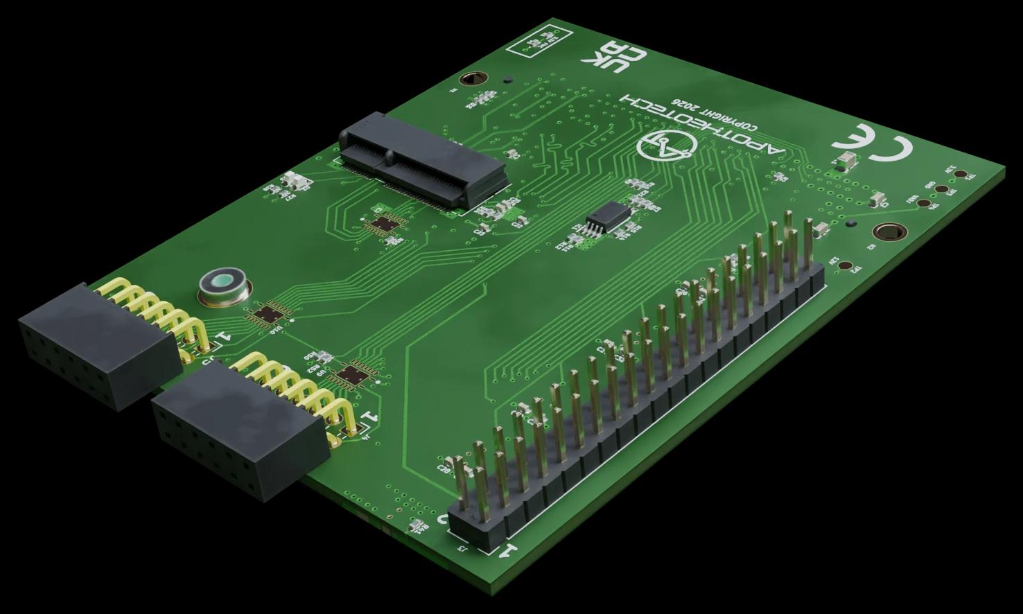
General-purpose I/O for an FPGA board with an FMC slot: a Raspberry Pi HAT-compatible 40-pin header, two PMOD connectors and an M.2 Key E slot on one card.

The 40-pin header takes existing Pi accessories directly. The two PMODs sit side by side for modules that need a dual-wide connection. The M.2 slot takes standard 2230 WiFi and Bluetooth modules over PCIe Gen2 x1 and USB 2.0. The I/O is level shifted and buffered.

Render to follow
Rates
SD, HD, 3G, 6G and 12G
Variants
4x RX, 4x TX, or 1x RX and TX
Waitlist

SDI FMC

APT-SDI-FMC-01

A multi-rate SDI card for broadcast and 4K/UHD video, up to 12G. It is in development in three variants: four receivers, four transmitters, or one of each.

It builds on the 12G-SDI receive, DMA and driver work from the 8-channel capture card project, and will come with reference designs including an SDI camera demo.

Software

The drivers and applications on the host side of the link. Most of this is still in development, and each entry says where it stands.

One Linux driver for every LitePCIe capture card, on x86 and Jetson AGX Orin. Frames arrive at /dev/video0, so standard V4L2 tools and applications work unchanged. Buffers are zero copy, and the DMA follows VSYNC so frames never tear.

Demosaic through color and tone, written on the CPU first for bit-exact checking and then ported to CUDA on the Jetson AGX Orin.

FPGA ISP stages

In development

Image processing stages that run in the FPGA between the sensor receiver and the link out, each configured over AXI4-Lite.

CamView

Running on hardware

A camera viewer and control application for CoaXPress hosts. It discovers, negotiates and locks the link, reads the camera's GenICam XML, builds its controls from it, then streams. It is used in the CoaXPress Host demos.

All software, with status

How buying works

IP cores are licensed per project

Each license is quoted on request. It is an encrypted netlist built for your device and configuration, with a basic example design, integration notes and one year of updates. Full reference designs, drivers and boards are sold separately.

Request a quote

Boards ship from the store

Boards are ordered in the store and paid for by card through Stripe. Setup guidance, documentation and hardware troubleshooting are included for 90 days after purchase.

Open the store

Changes and integration are project work

Integrating a core on your board, adding a feature the standard core leaves out, or building a full reference design around it is done as engineering services.

Engineering services

Not sure which part you need?

Say what the sensor is, how fast the data moves and where it has to go. We will tell you which core and board fit, or that none of them do.

Open the contact form

ApotheoTech LLC

Orlando, Florida

info@apotheotech.com